

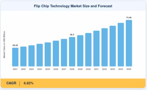
Flip Chip Technology Market Size Expected to Grow from USD 37.98 Billion in 2025 to USD 73.46 Billion by 2035
Flip Chip Technology Market
Flip Chip Technology Market Size, Share and Research Report By Wafer Bumping Process (Copper Pillar, Tin-Lead Eutectic Solder, Lead-Free Solder (SAC)
Flip Chip Technology Market is experiencing significant growth, supported by rising demand for high-performance semiconductor packaging in consumer electronics, automotive, AI, and 5G applications.”
LONDON, LONDON, UNITED KINGDOM, July 31, 2026 /EINPresswire.com/ -- The Global Flip Chip Technology market was valued at USD 37.98 billion in 2025 and is projected to reach USD 40.57 billion in 2026, growing to USD 73.46 billion by 2035 at a CAGR of 6.82% during the forecast period. This growth trajectory tracks the semiconductor industry's decisive shift toward chiplet-based system architectures, a transition catalyzed by over USD 52 billion in committed CHIPS Act funding across the United States and the European Chips Act's EUR 43 billion mobilization target. Foundry operators and outsourced assembly providers alike are racing to scale packaging capacity, and the Flip Chip Technology Market sits squarely at the center of that race, with AI and HPC packaging demand surge (~1.8% CAGR impact), chiplet and heterogeneous integration adoption (~1.4%), and high-bandwidth memory generational transitions (~1.2%) standing out as the highest-impact growth drivers.— Market Research Future (MRFR)
The technology landscape is undergoing a generational transition. Legacy wire-bonding and traditional solder bump processes are giving way to copper-pillar interconnects and, increasingly, Cu-to-Cu hybrid bonding architectures that deliver the sub-10 µm pitch densities demanded by AI accelerators and high-bandwidth memory stacks. Global capital expenditure on advanced packaging lines exceeded USD 8 billion in 2024, a figure expected to double by 2028 as hyperscale cloud operators contract directly with foundries for co-packaged optics and 2.5D/3D integration.
Asia-Pacific commands the dominant position, capturing approximately 57.8% of 2025 revenue, driven by concentrated OSAT capacity in Taiwan, South Korea, and mainland China, and is also the fastest-growing region at a projected 8.52% CAGR through 2035. North America holds the second-largest share at roughly 22.4%, underpinned by defense-grade packaging demand and CHIPS Act fab build-outs now materializing in Arizona, Ohio, and Texas, while Europe trails at approximately 12.8% share but is accelerating investment through its own semiconductor sovereignty programs.
Get Full PDF Sample Copy of Report: (Including Full TOC, List of Tables & Figures, Chart) @
https://www.marketresearchfuture.com/sample_request/5381
➤ How Significant Is the Flip Chip Technology Market's Growth?
The flip chip technology market's trajectory from USD 40.57 billion in 2026 to a projected USD 73.46 billion by 2035 represents nearly a 1.8-fold expansion over the forecast decade, reflecting the semiconductor industry's structural pivot from monolithic die scaling toward chiplet-based, heterogeneously integrated system architectures. The market's 6.82% CAGR is anchored in an AI-infrastructure supercycle where advanced packaging content per device is rising sharply as GPUs, AI accelerators, and high-bandwidth memory stacks demand ever-finer interconnect pitches.
Copper Pillar technology held a 49.2% revenue share in 2025, reflecting its dominance in high-density interconnect applications spanning server processors, networking ASICs, and mobile application processors, while Cu-to-Cu Hybrid Bonding is the fastest-expanding process segment, projected to grow at a 10.3% CAGR through 2035 as sub-5 µm pitch requirements accelerate adoption for next-generation HBM and logic-on-logic architectures.
FC-BGA led by packaging technology with a 40.4% share in 2025, driven by server-class processor packaging demand, while Fan-Out WLP and Panel-Level solutions are forecast to expand at a 10.7% CAGR as cost-optimized heterogeneous integration reaches mid-tier applications. Memory devices accounted for 34.2% of 2025 revenue by product, while GPU and AI Accelerator packaging is set to advance at a 13.4% CAGR, the fastest among product segments. Consumer Electronics & Wearables held a 31.1% share by end-use industry, while Data-Center & Cloud applications are expected to register an 8.56% CAGR through 2035.
➤ What Does the Future Hold for the Flip Chip Technology Market?
AI and HPC packaging demand surge is the single largest catalyst for the flip chip technology market, contributing approximately 1.8 percentage points to the CAGR. NVIDIA, AMD, and custom silicon programs at Google, Amazon, and Microsoft collectively consumed an estimated 2.4 million advanced-package units in 2024, a figure that grew over 60% year-on-year. Each next-generation GPU die whether NVIDIA's Blackwell or AMD's MI400 series requires larger interposer substrates with higher bump counts, directly expanding addressable flip chip content per device, with CoWoS and its equivalents now operating at near-full utilization across TSMC and ASE facilities.
Chiplet and heterogeneous integration adoption contributes approximately 1.4 percentage points to the CAGR: Intel's disaggregated Ponte Vecchio GPU contains over 40 chiplets bonded via EMIB and Foveros technology, while AMD's EPYC processors rely on multi-die flip chip assemblies, and the UCIe consortium's 1.1 specification status reached in 2024 is standardizing die-to-die interfaces and increasing the number of flip chip bonds per system by 3–5× compared with monolithic alternatives.
High-bandwidth memory generational transitions add a further 1.2 percentage points, as SK hynix, Samsung, and Micron are each investing over USD 10 billion cumulatively in HBM production capacity through 2027, with HBM4 expected to stack 16 DRAM layers and increase bump density by 40% versus HBM3E. Government semiconductor incentive programs contribute approximately 0.9 percentage points, with the U.S. CHIPS and Science Act allocating USD 39 billion in direct manufacturing incentives and Japan's METI committing JPY 3.9 trillion to semiconductor supply-chain resilience.
By 2030, an estimated 20–25% of all high-performance logic devices will ship as multi-chiplet assemblies, up from under 5% in 2024, as UCIe and other open interconnect standards create a modular chiplet ecosystem analogous to the PC component market's standardization era. Packages that co-locate compute, memory, and optical I/O on a single substrate will command premium pricing as global data-center electricity consumption is projected to exceed 1,000 TWh by 2030, and by 2035 non-Asia-Pacific advanced packaging capacity is expected to rise from 12% of the global total in 2024 to over 22%, reshaping competitive dynamics through more geographically distributed supply chains.
Get access to the full description of the report @
https://www.marketresearchfuture.com/reports/flip-chip-technology-market-5381
➤ Who Are the Key Players in the Flip Chip Technology Market?
The flip chip technology market exhibits medium concentration, with an estimated top-five share of 48–55% and a Herfindahl-Hirschman Index in the 900–1,200 range. The landscape features vertically integrated device manufacturers, pure-play foundries expanding into packaging, and dedicated OSAT providers, with competition intensifying as foundries like TSMC and Samsung bring advanced packaging in-house, compressing the addressable market for traditional OSATs. MRFR identifies the following key participants with estimated revenue share ranges:
★ ASE Technology Holding (~12–16% share) - the largest global OSAT, offering full-spectrum FC-BGA, 2.5D/3D, and copper-pillar bumping services, processing over 30% of the world's advanced packages.
★ Intel Corporation (~8–12% share) - an IDM with both captive and merchant packaging offering Foveros, EMIB, and hybrid bonding, and targeting volume glass-core substrate production by 2027.
★ TSMC (~7–11% share) - the foundry-led advanced packaging leader with CoWoS, InFO, and SoIC platforms; it announced a USD 100 billion U.S. investment plan in March 2025 including expanded CoWoS capacity in Arizona.
★ Amkor Technology (~7–10% share) - the second-largest OSAT and automotive-qualified specialist offering FC-BGA, FCCSP, and fan-out WLP; it broke ground on its first U.S. advanced packaging facility in Peoria, Arizona in July 2024.
★ Samsung Electronics (~6–9% share) - an IDM and foundry with HBM vertical integration through I-Cube and X-Cube platforms; it qualified its 12-layer HBM3E stack using advanced thermal compression bonding in September 2024.
★ JCET Group (~5–8% share) - the leading Chinese OSAT with a domestic supply-chain focus, offering FC-CSP, bumping, and 2.5D integration services.
★ Powertech Technology (~4–6% share) - a memory-centric OSAT aligned with Micron, providing memory packaging and bumping services.
★ TongFu Microelectronics (~3–5% share) - a Chinese OSAT scaling advanced packaging capability, offering FC-BGA and system-in-package solutions.
★ Chipbond Technology (~2–4% share) - a Taiwan-based niche bumping specialist providing bumping, gold stud, and testing services.
★ Texas Instruments (~2–4% share) - an IDM with captive analog packaging, offering flip chip solutions for analog and embedded applications.
Strategic competition in the flip chip technology market is increasingly defined by hybrid-bonding process maturity and yield, substrate supply-chain access, trusted-foundry defense accreditation, and the pace at which foundries' in-house packaging ambitions reshape OSAT pricing power and margin structure.
➤ What Are the Emerging Trends in the Flip Chip Technology Market?
Several transformational trends are redefining the flip chip technology market's evolution through 2035:
Co-Packaged Optics for Data Centers: Optical interconnects converging with flip chip packaging embed photonic engines within switch ASICs, providing power savings of up to 30% against pluggable transceivers, with Broadcom, Marvell, and Intel each developing CPO solutions representing a potential incremental USD 4+ billion opportunity by 2032.
Panel-Level Fan-Out Packaging: The move from round wafer-based to rectangular panel-based fan-out packaging is predicted to cut cost per unit area by 40–50%, with Samsung and Daedeok Electronics demonstrating panel-level FC-BGA substrate processing and industry roadmaps targeting volume production by 2027–2028.
Emerging Market Semiconductor Assembly Hubs: India's Semiconductor Mission, backed by USD 10 billion in government incentives, is attracting OSAT investment from Tata Electronics and CG Power, while Vietnam and Malaysia are similarly expanding packaging capabilities to de-risk concentrated APAC sourcing.
Automotive Chiplet Integration: Average semiconductor content per vehicle is expected to exceed USD 1,200 by 2030, up from roughly USD 700 in 2023, driving demand for automotive-grade flip chip packages in ADAS SoCs and power management ICs, despite 18–24 month qualification cycles.
AI-Driven Design and Process Optimization: Machine learning applied to flip chip design-rule optimization, bump placement, and defect detection is reducing design iterations by 25–30%, with Synopsys and Siemens EDA's AI-based layout tools creating a new recurring-revenue service layer for OSAT providers.
Sustainability and Green Packaging: Lead-free solder mandates under the EU's updated RoHS Directive and hyperscaler sustainability scorecards are pushing the market toward lower-impact processes, with hybrid bonding's elimination of solder materials positioning it as the most environmentally favorable interconnect technology at scale.
Buy Full Research Report:
https://www.marketresearchfuture.com/checkout?currency=one_user-USD&report_id=5381
➤ How Is the Flip Chip Technology Market Segmented?
The flip chip technology market report provides a comprehensive segmentation framework:
By Wafer Bumping Process: Copper Pillar (49.2% share, 2025), Tin-Lead Eutectic Solder (USD 8.42 Billion, 2025), Lead-Free Solder / SAC (5.62% CAGR), Cu-to-Cu Hybrid Bonding (10.3% CAGR), Gold Stud Bump (USD 1.84 Billion, 2025)
By Packaging Technology: FC-BGA (40.4% share, 2025), FCCSP / CSP (USD 9.18 Billion, 2025), Fan-Out WLP / Panel-Level (10.7% CAGR), 2.5D Interposer / CoWoS-type (9.86% CAGR), 3D Stacked (8.94% CAGR)
By Product: Memory DRAM, NAND, HBM (34.2% share, 2025), CMOS Image Sensor (USD 3.62 Billion, 2025), CPU / MPU (6.48% CAGR), GPU / AI Accelerator (13.4% CAGR), Networking / Switch ASIC (7.82% CAGR), PMIC / Analog (USD 2.94 Billion, 2025)
By End-Use Industry: Consumer Electronics & Wearables (31.1% share, 2025), Data-Center & Cloud (8.56% CAGR), Automotive & Transportation (9.24% CAGR), Industrial & Robotics (USD 4.28 Billion, 2025), Telecommunications (6.74% CAGR), Aerospace & Defense (USD 2.16 Billion, 2025)
By Region: Asia-Pacific (57.8% share, 2025), North America (USD 8.51 Billion, 2025), Europe (6.38% CAGR), South America (USD 1.52 Billion, 2025), Middle East & Africa (5.18% CAGR)
➤ What Are the Regional Insights from the Flip Chip Technology Market?
Asia-Pacific leads the flip chip technology market with 57.8% of 2025 revenue, reflecting the region's unmatched OSAT concentration. China commands approximately 32.4% of regional revenue through domestic OSAT expansion and HiSilicon demand, South Korea contributes through Samsung and SK hynix's massive thermal-compression-bonding capacity for HBM production, and India is expanding at a 9.14% CAGR through Semiconductor Mission greenfield investments, while Japan and ASEAN contribute through Rapidus and legacy OSAT modernization and Malaysia/Vietnam assembly diversification respectively. Taiwan-based ASE Technology Holding alone processes over 30% of the world's advanced packages.
North America holds approximately USD 8.51 billion in 2025 revenue, with the United States accounting for 78.4% of regional share through Intel's USD 20 billion Ohio fab complex, TSMC's Arizona facility ramping 4/3 nm production with adjacent CoWoS capacity, and a dense cluster of defense-grade OSAT providers serving Department of Defense trusted-foundry programs. Canada is growing at a 5.22% CAGR through photonics and quantum packaging R&D at institutions such as the National Research Council, while Mexico is emerging as a low-cost back-end assembly hub for consumer electronics OEMs.
Europe is growing at a 6.38% CAGR, anchored by Germany's 28.6% of regional revenue through automotive semiconductor sovereignty, where Infineon, Bosch, and Continental drive demand for automotive-qualified flip chip packages. The European Chips Act's Pilot Line initiative is funding advanced packaging R&D at IMEC in Belgium and Fraunhofer IZM in Germany focused on 3D heterogeneous integration, while the UK, France, Italy, Spain, and the Nordic countries contribute through compound semiconductor packaging, STMicroelectronics and CEA-Leti R&D, power semiconductor packaging, emerging OSAT partnerships, and RF and sensor packaging respectively.
South America and the Middle East & Africa represent smaller but developing shares of global revenue. Brazil dominates South America with 62.5% of regional revenue, primarily through EMS operations assembling consumer devices under Manaus free-trade-zone incentives, while Argentina contributes through government digital infrastructure programs. In the Middle East & Africa, Saudi Arabia holds 31.8% of regional revenue through Vision 2030 digital economy programs including semiconductor design centers and international foundry partnerships, the UAE is expanding at a 6.02% CAGR through smart-city semiconductor procurement, and South Africa and Egypt contribute through mining and industrial IoT packaging demand and electronics manufacturing localization respectively.
➤➤➤ Regional & Country-Level Reports by Market Research Future:
US Flip Chip Technology Market -
https://www.marketresearchfuture.com/reports/us-flip-chip-technology-market-16409
➤➤➤ Related Reports by Market Research Future:
Magnetic Proximity Sensors Market
https://www.marketresearchfuture.com/reports/magnetic-proximity-sensors-market-42812
High End Imu Market
https://www.marketresearchfuture.com/reports/high-end-imu-market-42817
Sensor Fusion In Autonomous Vehicle Market
https://www.marketresearchfuture.com/reports/sensor-fusion-in-autonomous-vehicle-market-42848
Inductors Cores And Bead Market
https://www.marketresearchfuture.com/reports/inductors-cores-and-bead-market-42849
Medium Voltage Electric Drives Market
https://www.marketresearchfuture.com/reports/medium-voltage-electric-drives-market-42861
Binder Jetting 3D Printing Technology Market
https://www.marketresearchfuture.com/reports/binder-jetting-3d-printing-technology-market-42869
Ultra Large Scale Ic Market
https://www.marketresearchfuture.com/reports/ultra-large-scale-ic-market-42877
Thermography Condition Monitoring Equipment Market
https://www.marketresearchfuture.com/reports/thermography-condition-monitoring-equipment-market-42882
Semiconductor Applications In Healthcare Market
https://www.marketresearchfuture.com/reports/semiconductor-applications-in-healthcare-market-42885
It Connector Market https://www.marketresearchfuture.com/reports/it-connector-market-42892
Sagar Kadam
Market Research Future
+ + +1 628-258-0071
email us here
Legal Disclaimer:
EIN Presswire provides this news content "as is" without warranty of any kind. We do not accept any responsibility or liability for the accuracy, content, images, videos, licenses, completeness, legality, or reliability of the information contained in this article. If you have any complaints or copyright issues related to this article, kindly contact the author above.
